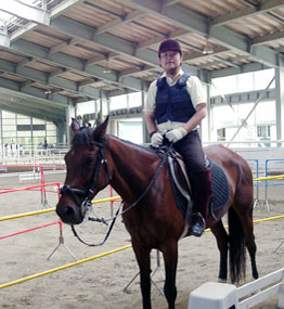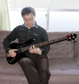


I was born in Hikone, Japan in 1961.
I received the B.E., the M.E. and the Ph.D degree from Nagoya Institute of Technology, Nagoya, Japan in 1985, 1987 and 1991, respectively. Since 1989 I worked for the Department of Electrical and Computer Engineering, Kanazawa University, Japan. From 1997 to 1998, I went abroad to study in Microsystems Technology Labratories, Massachusetts Institute of Technology (MIT). Since 1999 I transferred to VLSI Design and Education Center (VDEC), The University of Tokyo, Japan. From 2001 to 2003, I had been with the Department of Information and Systems Engineering, Kanazawa University, Japan. From 2004 to 2007, I had been with Division of Electrical Engineering and Computer Science, Graduate School of Natural Science and Technology, Kanazawa University. Since 2008 I am working for College of Science and Engineering, School of Electrical, Information and Communication Engineering in Kanazawa University. I left Kanazawa University and have started SMeRL(Sensor-Microelectronics Research Lab.) as a sole proprietor in 2025.
My research interests include a phase change nonvolatile RAM, mixed signal VLSI design, sensor network for IoT, microelectronics for energy harvesting, and psychological effects of mixed reality.
I am a member of the Institute of Electrical and Electronics Engineers (IEEE).